Nova 200 NanoLab: SEM & EDS: Difference between revisions
Jump to navigation
Jump to search
No edit summary |
No edit summary |
||
| Line 58: | Line 58: | ||
* [https://caltech.box.com/s/tlqgvtkkiahi261megm087i61gqlfzrc Scripting – RunScript Manual] | * [https://caltech.box.com/s/tlqgvtkkiahi261megm087i61gqlfzrc Scripting – RunScript Manual] | ||
===== Simulation Software ===== | ===== Simulation Software ===== | ||
* [http://www.gel.usherbrooke.ca/casino/What.html CASINO Electron Beam Simulation Software – simulate e-beam/specimen interactions | * [http://www.gel.usherbrooke.ca/casino/What.html CASINO Electron Beam Simulation Software] – simulate e-beam/specimen interactions | ||
* [http://www.srim.org/ The Stopping & Range of Ions in Matter (SRIM) – simulate i-beam/specimen interactions | * [http://www.srim.org/ The Stopping & Range of Ions in Matter (SRIM)] – simulate i-beam/specimen interactions | ||
===== Order Your Own Stubs ===== | ===== Order Your Own Stubs ===== | ||
* Stubs used for mounting specimens are considered a personal, consumable item in the KNI. There are some old stubs at each SEM, yet you should buy your own so that you can keep them clean and available to you. There are many stub geometries and configurations, some of which will be right for you to purchase and keep with your other cleanroom items. | * Stubs used for mounting specimens are considered a personal, consumable item in the KNI. There are some old stubs at each SEM, yet you should buy your own so that you can keep them clean and available to you. There are many stub geometries and configurations, some of which will be right for you to purchase and keep with your other cleanroom items. | ||
** [https://www.tedpella.com/SEM_html/SEMclip.htm.aspx Buy stubs with copper clips (recommended for most devices, | ** [https://www.tedpella.com/SEM_html/SEMclip.htm.aspx Buy stubs with copper clips] (recommended for most devices, especially those with non-conductive substrates) | ||
** [https://www.tedpella.com/sem_html/SEMpinmount.htm Buy stubs without copper clips ( | ** [https://www.tedpella.com/sem_html/SEMpinmount.htm Buy stubs without copper clips] (OK for devices with conductive substrates) | ||
== Specifications == | == Specifications == | ||
Revision as of 22:36, 24 April 2019
|
Description
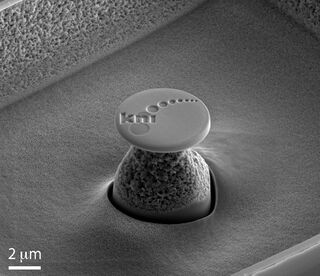
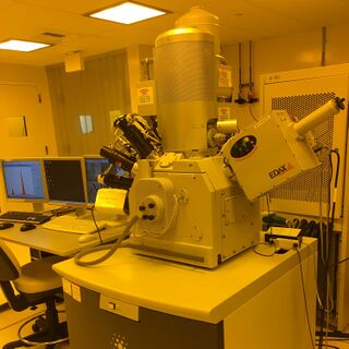
The Nova 200 is the KNI's highest-resolution analytical scanning electron microscope (SEM), equipped with an immersion-lens for imaging sub-10 nm features and both energy dispersive spectroscopy (EDS) and wavelength dispersive spectroscopy (WDS) detectors for compositional analysis. It is also outfitted with a gallium focused ion beam (Ga-FIB) column, which is currently not operational because the Nova 600 NanoLab and ORION NanoFab together meet the KNI's Ga-FIB demand; gallium could be reactivated on the Nova 200 the future. See a full list of training and educational resources for this instrument below.
SEM Applications
- Ultra-High-Resolution Imaging (Immersion Mode)
- High-Resolution Imaging (Field-Free Mode)
- Secondary Electron (SE) & Backscattered Electron (BSE) Imaging
- Everhart-Thornley Detector (ETD) & Through-the-Lens Detector (TLD)
- Tungsten deposition via Gas Injection System (GIS)
- Automated imaging with RunScript program & AutoScript language
Analytical Applications
- Compositional analysis with EDS (via x-ray detection)
- Compositional analysis with WDS (via x-ray detection)
Resources
SOPs & Troubleshooting
- SEM SOPs (Short Version | Long Version)
- Ga-FIB SOPs (Short Version | Long Version)
- TEM Lamella Sample Preparation SOPs (Short Version | Long Version)
- Cutting & Imaging Cross-Sections SOP
- Troubleshooting Guide
Video Tutorials
- Getting Started | Basic SEM Alignment
- Astigmatism Correction (Details | On Right-Angle Features | Stigmator Alignment)
- Eucentric Height: What it means, When to use it & How to get there
- Adjusting TLD Voltage to Capture SE vs. BSE Signal
Graphical Handouts
Presentations
Manufacturer Manuals
- Nova NanoLab Operation Manual
- Gas Injection Systems – Deposition of Platinum (Technical Note)
- Gas Injection Systems – Deposition of SiOx (Technical Note)
- Gas Injection Systems – Etching with IEE aka XeF2 Etch (Technical Note)
- Gas Injection Systems – Beam Chemistries Presentation
- Scripting – AutoScript Language Manual (year 2000 Technical Note: most complete)
- Scripting – AutoScript Language Manual (year 2005 Technical Note: less complete, still useful)
- Scripting – RunScript Manual
Simulation Software
- CASINO Electron Beam Simulation Software – simulate e-beam/specimen interactions
- The Stopping & Range of Ions in Matter (SRIM) – simulate i-beam/specimen interactions
Order Your Own Stubs
- Stubs used for mounting specimens are considered a personal, consumable item in the KNI. There are some old stubs at each SEM, yet you should buy your own so that you can keep them clean and available to you. There are many stub geometries and configurations, some of which will be right for you to purchase and keep with your other cleanroom items.
- Buy stubs with copper clips (recommended for most devices, especially those with non-conductive substrates)
- Buy stubs without copper clips (OK for devices with conductive substrates)
Specifications
Manufacturer Specifications
- Nova 600 NanoLab Data Sheet (not all parameters apply to our instrument, see below for details specific to the KNI's Nova 600)
Scanning Electron Microscope (SEM) Specifications
- 0.5 to 30.0 kV
- Apertures: 10 mm, 15 mm, 20 mmm, 30 mm
- etc.
Gallium Focused Ion Beam (Ga-FIB) Specifications
- 5.0 to 30.0 kV
- 10 pA - 20 nA
- etc.

