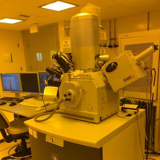
Nova 200 NanoLab: SEM & EDS: Difference between revisions
Jump to navigation
Jump to search
m (Removed link to Equipment Status under Resources since the status can be viewed directly by users in FBS, per Tiffany 4/15/24 sg) |
|||
| Line 33: | Line 33: | ||
== Resources == | == Resources == | ||
===== SOPs & Manuals & SDS ===== | ===== SOPs & Manuals & SDS ===== | ||
* [https://caltech.box.com/s/ | * [https://caltech.box.com/s/rpbtox8l31qi3kw3b014e3e8i4ctjpdy KNI Microscopy Policies] | ||
* [https://caltech.box.com/s/4f1hqp83pwc1v1k5qke6xi68i28fjvz8 Nova200 and EDS SOP, Manuals, SDS] | * [https://caltech.box.com/s/4f1hqp83pwc1v1k5qke6xi68i28fjvz8 Nova200 and EDS SOP, Manuals, SDS] | ||
* [https://caltech.box.com/s/og4309108q4k2jwhkaxqtpiujg2al5iu Nova NanoLab Operation Manual] | * [https://caltech.box.com/s/og4309108q4k2jwhkaxqtpiujg2al5iu Nova NanoLab Operation Manual] | ||
Latest revision as of 22:35, 5 February 2025
|
Description
The Nova 200 is the KNI's highest-resolution field-emission gun (FEG) analytical scanning electron microscope (SEM), equipped with an immersion lens for imaging sub-10 nm features and energy dispersive spectroscopy (EDS) for compositional analysis. It is also outfitted with a gallium focused ion beam (Ga-FIB) column, which is currently not operational because the Nova 600 NanoLab and ORION NanoFab together meet the KNI's Ga-FIB demand; Ga-FIB could be reactivated on the Nova 200 in the future. See a full list of training and educational resources for this instrument below.
SEM Applications
- Ultra-High-Resolution Imaging (Immersion Mode aka UHR Mode)
- High-Resolution Imaging (Field-Free Mode aka Normal Mode)
- Secondary Electron (SE) imaging with an Everhart-Thornley Detector (ETD) & Through-the-Lens Detector (TLD)
- Backscattered Electron (BSE) imaging with a TLD
- Tungsten deposition via Gas Injection System (GIS)
- Automated imaging with RunScript program & AutoScript language
EDS Applications
- Spectrum acquisition for qualitative and quantitative compositional analysis
- Linescan acquisition for 1D spatial compositional analysis
- Map acquisition for 2D spatial compositional analysis
Resources
SOPs & Manuals & SDS
- KNI Microscopy Policies
- Nova200 and EDS SOP, Manuals, SDS
- Nova NanoLab Operation Manual
- Bruker Quantax EDS Operation Manual
- Gas Injection Systems – Deposition of Tungsten (Technical Note)
- Gas Injection Systems – Delineation Etch for SiO2 (Technical Note)
- Gas Injection Systems – Selective Carbon Etching (Technical Note)
- Scripting – AutoScript Language Manual (year 2000 Technical Note: most complete)
- Scripting – RunScript Manual
Video Tutorials
- Getting Started | Basic SEM Alignment
- Astigmatism Correction (Details | On Right-Angle Features | Stigmator Alignment)
- Adjusting TLD Voltage to Capture SE vs. BSE Signal
- Bruker EDS ESPRIT 2 Software (Overview | Basic Spectrum Collection and ID | Spectrum Acquisiton | AutoID Verification | Object Mode (Multi-Point Analysis) | Line Profile Analysis)
Graphical Handouts
Presentations
- SEM Essentials: Capabilities and Limitations of Scanning Electron Microscopy; and SEM Setup, Parameters and Theory for Successful Operations and Measurements
- Scanning Electron Microscopy: Principles, Techniques & Applications
- Gallium Focused Ion Beam Microscopy: Principles, Techniques & Applications
Simulation Software
- CASINO Electron Beam Simulation Software – simulate e-beam/specimen interactions (very useful for EDS & WDS)
- The Stopping & Range of Ions in Matter (SRIM) – simulate i-beam/specimen interactions
Calibrate Measurements with NIST Standard
- The KNI has a NIST-traceable standard against which SEM measurements can be compared. See Slides 54-55 of the SEM Presentation for details. Ask staff for help finding and using the standard in the lab.
Sample Preparation
- Use the Carbon Evaporator to make non-conductive samples conductive by applying 2-10 nm of evaporated carbon.
- Use the O2/Ar Plasma Cleaner to remove hydrocarbons from the sample surface to avoid creating dark contamination spots on your features while imaging them.
Stubs for specimen mounting
- Stubs used for mounting specimens are considered a personal, consumable item in the KNI. There are some stubs at each Microscope which can be used by any KNI microscopy user. You can also buy your own stubs so that you can keep them clean and available to you. There are many stub geometries and configurations. If you chose to buy your own stubs, please show them to the staff microscopist prior to using them: some stubs including stubs with copper clips have large height differences and can only be used safely in specific operating conditions.
Guide to Choosing KNI SEMs & FIBs
Specifications
Manufacturer Specifications
- Nova 200 NanoLab Data Sheet (not all parameters apply to our instrument, see below for details specific to the KNI's Nova 200)
SEM Specifications
- Minimum Feature Size Resolved in Immersion Mode: ~5 nm
- Voltage Range: 0.2 to 30.0 kV
- Current Range: ~10 pA to 20 nA
- Apertures: 30 μm, 40 μm, 50 μm, 100 μm
- Eucentric Height: ~4.8 mm working distance (WD)
- Stage Range: ±25 mm X & Y travel, 50 mm Z travel, -12 to 58° tilt, 360° rotation
- ETD Grid Bias Range: -150 to 300 V
- TLD Bias Range: -100 to 150 V
- Ultimate Vacuum: 5e-6 mbar
