Contact Mask Aligners: MA6 & MA6/BA6: Difference between revisions
Jump to navigation
Jump to search
No edit summary |
|||
| Line 69: | Line 69: | ||
* Channel 1 is 365nm wavelength at 10 mW/cm2. | * Channel 1 is 365nm wavelength at 10 mW/cm2. | ||
* Channel 2 is 405nm wavelength at 15 mW/cm2. | * Channel 2 is 405nm wavelength at 15 mW/cm2. | ||
== Related Instrumentation in the KNI == | |||
===== Electron Beam Lithography ===== | |||
* [[EBPG 5200: 100 kV Electron Beam Lithography|EBPG 5200: 100 kV Electron Beam Lithography]] | |||
* [[EBPG 5000+: 100 kV Electron Beam Lithography | EBPG 5000+: 100 kV Electron Beam Lithography]] | |||
* [[Quanta 200F: SEM, ESEM, Lithography & Probe Station | Quanta 200F: SEM with 1-30 kV Electron Beam Lithography]] | |||
* [[Tecnai TF-20: 200 kV TEM, STEM, EDS, EELS, EFTEM & Lithography | Tecnai TF-20: TEM & STEM with 80-200 kV Electron Beam Lithography]] | |||
===== Ion Beam Lithography ===== | |||
* [[ORION NanoFab: Helium, Neon & Gallium FIB | ORION NanoFab: Helium (5-40 kV), Neon (5-35 kV) & Gallium (1-30 kV) Focused Ion Beam Lithography & Microscopy]] | |||
===== Optical Lithography ===== | |||
* [[Wafer Stepper | i-Line Wafer Stepper: GCA model 6300]] | |||
* [[CNI-PV 2.1: Nano Imprint Lithography | Nano Imprint Lithography: NILT CNI-PV 2.1]] | |||
* [[DWL-66: Direct-Write Laser System | Direct-Write Laser System: Heidelberg Instruments DWL-66]] | |||
* [[Nanoscribe PPGT: Microscale 3D Printer | Two-Photon Lithography (aka Microscale 3D Printing): Nanoscribe Photonic Professional GT]] | |||
* [[Optical Lithography Resources]] | |||
Revision as of 16:34, 12 October 2020
|
Description
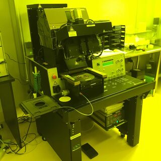
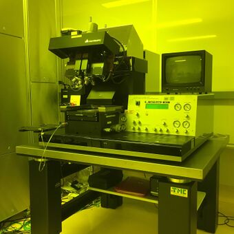
The contact mask aligner is a tool that enables front- and back-side alignment of photo masks to create structures as small as 500 nm on sample sizes up to 6 inches. These systems are ideally suited for rapid definition of sub-micron devices through contact printing, and enable the high-resolution alignment of several lithographic layers to define complex devices. They are typically used to define contacts and connections to the nanostructures that are defined using the KNI's other fabrication instruments (e.g. e-beam lithography). The MA6/BA6 is also configured to do bond aligning in support of the Suss Microtec SB6L Wafer Bonder.
Suss1 MA6/BA6 Applications
- Front Side Flood Exposure (no mask)
- Front Side Alignment & Exposure
- Back Side Alignment with Front Side Exposure
Suss2 MA6 Applications
- Front Side Alignment & Exposure
- Back Side Alignment with Front Side Exposure
Resources
Equipment Data
SOPs & Troubleshooting
- General SOP & Troubleshooting
- Lamp Change SOP
- Lamp Re-Ignition SOP
- Suss 1 Lamp Re-Ignition Video
- Suss 2 Lamp Re-Ignition Video
Optical Lithography Resources
- Optical Lithography Resources Page
- Laurell Spinner Cleaning SOP
- Laurell Spinner - Spinning Resist Video
Process Recipes
Manufacturer Manuals
- Suss MA6/BA6 System Manual
- Suss MA6/BA6 Brochure
- Lamp Power Supply Manual
- Alignment Mark Suggestion Document
Specifications
Manufacturer Specifications
- Whole wafers 2” up to 6” can be loaded.
- Samples pieces up to 6”x6” square can be loaded.
- Samples up to 6mm thick can be loaded..
- Exposure Resolution:
- Soft Contact Mode = 1 - 2 um
- Hard Contact Mode = 1 um
- Soft Vacuum Contact Mode = 1 - 0.5 um
- Vacuum Contact Mode = 0.4 - 0.5 um
Suss 1 Exposure Settings
- Channel 1 is 365nm wavelength at 15 mW/cm2.
- Channel 2 is 405nm wavelength at 25 mW/cm2.
Suss 2 Exposure Settings
- Channel 1 is 365nm wavelength at 10 mW/cm2.
- Channel 2 is 405nm wavelength at 15 mW/cm2.
Related Instrumentation in the KNI
Electron Beam Lithography
- EBPG 5200: 100 kV Electron Beam Lithography
- EBPG 5000+: 100 kV Electron Beam Lithography
- Quanta 200F: SEM with 1-30 kV Electron Beam Lithography
- Tecnai TF-20: TEM & STEM with 80-200 kV Electron Beam Lithography

