Spectroscopic Ellipsometer: Difference between revisions
Jump to navigation
Jump to search
No edit summary |
No edit summary |
||
| (One intermediate revision by the same user not shown) | |||
| Line 32: | Line 32: | ||
** [https://youtu.be/54w-i0R4SMA Part 2: Transparent polymers] | ** [https://youtu.be/54w-i0R4SMA Part 2: Transparent polymers] | ||
** [https://youtu.be/l6-uTJ-V3EU Part 3: Absorbing Films via B-Spline] | ** [https://youtu.be/l6-uTJ-V3EU Part 3: Absorbing Films via B-Spline] | ||
** [https://youtu.be/grQ1izdiT4A Part 4: Modeling Absorption with Oscillators] | |||
** [https://youtu.be/EY7wKNnstMw Part 5: Thickness Measurement of Metals] | |||
== Specifications == | == Specifications == | ||
Latest revision as of 23:48, 30 March 2020
|
Description
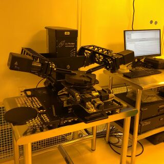
The J.A. Woolam M-2000 spectroscopic ellipsometer is a tool for optical thin film analysis that enables determination of thickness, optical constants n and k (refractive index and absorption coefficient), and allows modeling of electronic characteristics such as majority carrier concentration and band-gap. The beam incidence angle ranges from 45-90°, allowing both standard ellipsometry and transmission measurements. It is equipped with a motorized sample stage that enables wafer-scale measurements. The CompleteEASE control and analysis software possesses detailed measurement and modeling capability.
Applications
- Thickness measurement
- Optical & electronic property analysis
- Surface roughness measurement
- Materials identification
Resources
SOP
Video Tutorials
- Ellipsometry & CompleteEASE:
Specifications
Hardware Specifications
- CompleteEASE measurement and analysis software
- Spectral Range: 370-1000 nm
- Motorized stage enables automated mapping scans across up to 100 mm wafers
- Automatic measurement angle control
- Automatic sample alignment
- 2 mm spot size
- Removable beam focusing probes can reduce spot size to 300 μm
