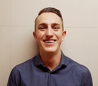
Evan Piano: Difference between revisions
No edit summary |
No edit summary |
||
| Line 12: | Line 12: | ||
== About == | == About == | ||
===== Role in the KNI ===== | ===== Role in the KNI ===== | ||
Evan is the Nanofabrication Process Engineer for The Kavli Nanoscience Institute (KNI) at the California Institute of Technology. Evan joined the KNI through Waterloo's renowned co-op program, | Evan is the Nanofabrication Process Engineer Intern for The Kavli Nanoscience Institute (KNI) at the California Institute of Technology. Evan has joined the KNI through Waterloo's renowned co-op program. Over an eight-month period from January to August 2020, he will be working – both independently and alongside KNI staff – on nanofabrication process recipe development, characterization, and documentation across all areas of the lab. He will be primarily focusing his efforts on reactive-ion etching (RIE), electron beam lithography (EBL), physical & chemical vapor deposition (PVD & CVD), and wet chemistry. | ||
===== Education ===== | ===== Education ===== | ||
Evan is a fourth year undergraduate student at the University of Waterloo where he studies Nanotechnology Engineering. He has microfabrication cleanroom experience working on equipment and techniques such as | Evan is a fourth year undergraduate student at the University of Waterloo where he studies Nanotechnology Engineering. He has microfabrication cleanroom experience working on equipment and techniques such as photolithography, RIE, PECVD, AFM, SEM, and ellipsometry, from his previous positions held at the Centre for Advanced Photovoltaics and Display Systems, NAV Canada, and Centra Industries (a division of PCC Aerostructures). | ||
Revision as of 21:43, 21 January 2020
|
About
Role in the KNI
Evan is the Nanofabrication Process Engineer Intern for The Kavli Nanoscience Institute (KNI) at the California Institute of Technology. Evan has joined the KNI through Waterloo's renowned co-op program. Over an eight-month period from January to August 2020, he will be working – both independently and alongside KNI staff – on nanofabrication process recipe development, characterization, and documentation across all areas of the lab. He will be primarily focusing his efforts on reactive-ion etching (RIE), electron beam lithography (EBL), physical & chemical vapor deposition (PVD & CVD), and wet chemistry.
Education
Evan is a fourth year undergraduate student at the University of Waterloo where he studies Nanotechnology Engineering. He has microfabrication cleanroom experience working on equipment and techniques such as photolithography, RIE, PECVD, AFM, SEM, and ellipsometry, from his previous positions held at the Centre for Advanced Photovoltaics and Display Systems, NAV Canada, and Centra Industries (a division of PCC Aerostructures).
