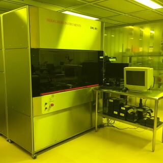
DWL-66: Direct-Write Laser System: Difference between revisions
Jump to navigation
Jump to search
No edit summary |
(→SOPs) |
||
| Line 24: | Line 24: | ||
== Resources == | == Resources == | ||
===== SOPs ===== | ===== SOPs ===== | ||
* [https://caltech.box.com/s/miia23ob94wsdomfb2bi00d4cfhdeuao | * [https://caltech.box.com/s/miia23ob94wsdomfb2bi00d4cfhdeuao Operation SOP] | ||
===== Manufacturer Manuals ===== | ===== Manufacturer Manuals ===== | ||
* [https://caltech.box.com/s/kvh2lwhzq6gzd12a43a5nr1xv0hrwb8p User Guide, Part 1] | * [https://caltech.box.com/s/kvh2lwhzq6gzd12a43a5nr1xv0hrwb8p User Guide, Part 1] | ||
Revision as of 21:00, 28 May 2019
|
Description
The Heidelberg Instruments DWL-66 is a tool for mask making and for direct patterning of wafers by the use of a HeCd laser. Precise control of the laser head and alignment produces 800-nm resolution lithography. The DWL 66 is an extremely high-resolution imaging system where over half a million dpi (dots per inch) is achieved using a 40-nm writeable address grid for exposing chrome plates or wafers.
Applications
- Direct Writing
- Grayscale Writing
Resources
SOPs
Manufacturer Manuals
Specifications
- Exposure: 442 nm wavelength HeCd laser
